The structure chemical states electrical and optical properties of the films have been investigated with tungsten-doping content and annealing temperature. The dopant-induced changes in MOS materials used in the gas sensing are also elaborated in the paper.

Pdf Electrical And Optical Properties Of Tin Thin Films
Before characterization the ITO films were annealed at different temperatures ranging from 100 to 500 deg.
Electrical and optical properties of tin thin films. A sheet resistance of 14-17 Ωsquare units were obtained for as-deposited CdOSn thin films with a thickness of 120-150 nm. In this paper FTO thin film on glass substrate has been prepared by spray pyrolysis technique and discussed its optical and electrical properties for first time in terms of the Drude-Lorentz model that to the best of our knowledge it is also the first time that both properties of. The present study reveals the effect of dopant atoms to the structural and optical properties as well as the selectivity and sensitivity for particular metal oxides semiconductor and few semiconductor thin films.
The films of PbS have direct band gap I68 - 232 ev at 300 K the values of band energy decreases with increases thickness of the Lead II Sulfide films. The optical properties of the TiN thin films have been investigated. From our data we cannot demonstrate the relationship between oxygen vacancies and ultra-thin ITO electrical properties.
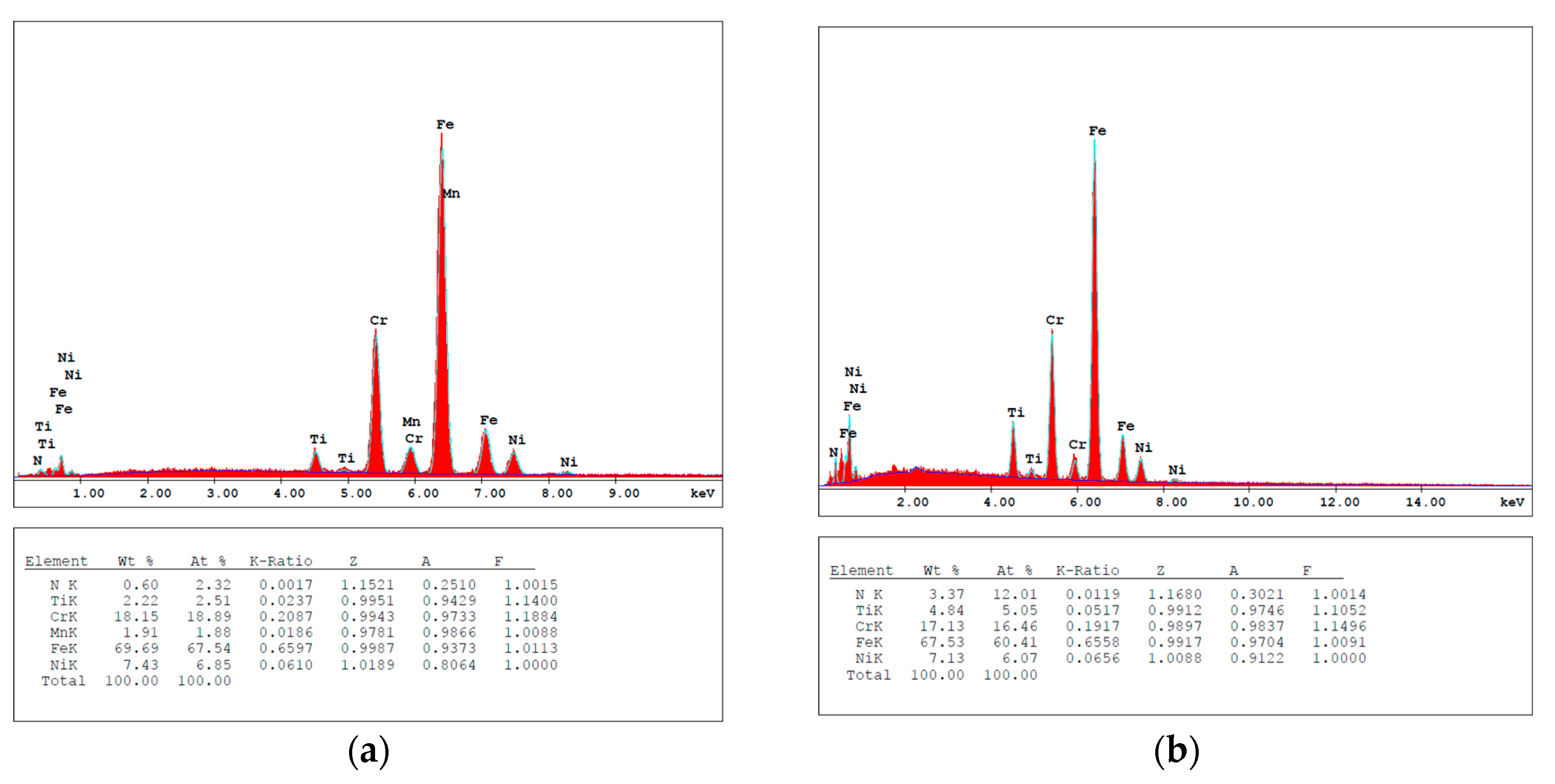
The structural electrical and optical properties of the fabricated thin films were influenced by partial pressure of Dimethylcadmium and Tetramethyltin substrate temperature film thickness and annealing conditions. The analysis of the chemical compositions for the as-deposited as well as annealed ZnTe thin films was estimated by using the method of energy dispersive analysis of x-ray EDAX. The activation energy for conduction in the TiN films at temperatures in the range 295 K T 420 K is 015 eV.
UVVisible spectrometer analysis showed excellent optically transparent oscillating natures with transparency above 85 in the visible range. The TiN thin films have been shown to be n -type semiconductors with a carrier concentration of 288 10 22 cm 3 and resistivity of ρ 04 Ω cm at room temperature. The positive sign of the power under dark conditions indicates dissipation of the power in the TiNO while the negative sign of the power under the visible light illumination indicates the power generation capability of the TiNO.
Electrical and optical properties of ITO films. The thin films were successfully deposited by thermal evaporation using Edwards Auto 306 Magnetron Sputtering System. The optimized conditions resulted in a thin film with average visible transmittance of 83 and optical band-gap of 380 eV resistivity of 671 10 3 Ωcm a carrier concentration N d.
Tin Selenide SnSe thin films were prepared from the pulverized compound material by thermal evaporation method to study the effect of film thickness on its structural and optical properties. In this paper indium oxide In 2 O 3 thin films are prepared by plasma-enhanced atomic layer deposition PEALD using cyclopentadienylindiumI InCp as the metal precursor and O 2 plasma as the oxidant. Electrical optical and structural properties of tin doped ZnO thin films were investigated for various tin Sn doping concentrations.
Among TCO thin films indium tin oxide ITO thin film has been almost exclusively used in optoelectronic devices due to its higher transmittance in the visible region and lower electrical properties. The thin film produced was polycrystalline with a tetragonal crystal structure. The optical properties of the TiN thin films have been investigated.
Optical properties showed that the thin films have high transmission at visible range and low transmission at UV IR range. The structural electrical and optical properties of these films have been investigated as a function of target composition substrate deposition temperature background gas pressure and film thickness. ITO thin films onto glass substrates are widely used as transparent and conductive electrodes.
Band gap of 324 eV. The different thicknesses of SnSe thin films from 150 nm to 500 nm were grown on glass substrate held at room temperature. For all as-grown NBSO thin films the optical transmittance in the visible wavelength region is larger than 80.
The detailed analysis of the electrical properties of the thin film as a function of the fluorine doping level revealed that a resistivity as low as 671 10 3 Ωcm was obtained with a fluorine content of 53 at. The mechanism and effects of annealing temperature under the air atmosphere on optical structural and electrical properties of the films are investigated. The best sample was observed at 1 oxygen with the sheet resistance of 227 Ω resistivity of 56x10-4 Ωcm and transmittance at 550 nm of 73.
High-quality indiumtinoxide ITO thin films 200850 nm have been grown by pulsed laser deposition PLD on glass substrates without a postdeposition annealing treatment. The material of the TiN thin films has been shown to be a direct gap semiconductor with a band gap Eg 34 eV. C for a constant time of 15 min in air.
En Radio frequency rf-sputtered indium tin oxide ITO thin films were characterized by studying their structure electrical and optical properties. The substrate temperature affects strongly on the surface morphology and electrical properties of ITO films. A ternary TiNO material system has been synthesized in thin film form that exhibits properties that neither of the two binary parent compounds TiN and TiO 2 possess.
It was also reported that electrical properties of ultra-thin ITO films can be improved by reducing the number of damaging high energy particles and at the same time having an optimal negative oxygen ions to generate more oxygen vacancies without altering ITO stoichiometry 16 30. 4 rows The electrical and optical properties of amorphous indium zinc tin oxide a-IZTO thin. Electrical optical and structural properties of tin doped ZnO thin films were investigated for various tin Sn doping concentrations.
The lowest resistivity of 667 10 4 Ω cm was obtained with carrier mobility of 65 cm 2 V 1 s 1 and carrier concentration of 144 10 20 cm 3 in 3 wt tungsten-doping films annealed at 800 C in air. The morphological structural optical and electrical properties were studied. Sol gel method was used to deposit the films on microscopic glass slides and silicon substrate.
The thin films of undoped tin oxide SnO 2 were deposited onto the amorphous glass substrates. Their optical and electrical properties were studied using Solid Spec-3700 DUV Spectrophotometer and Four Point Probe method respectively. Tin Selenide SnSe thin films were optimised for thin film solar cell applications.
Sol gel method was used to deposit the films on microscopic. X-ray diffraction atomic force microscopy transmission measurement and. The average optical transmittance achieved for this coating was 83 across a range of 300 λ 900 nm.
The optimized comprehensive properties of the NBSO films with FWHM 011 ρ 05 mΩ cm μ 249 cm2Vs and T 80 are superior to those of other rare-earth and 4d- and 5d-transition metal-doped BaSnO3 thin films. Zinc Telluride ZnTe thin films were deposited onto glass and CdTe substrates by CSVT Close Space Vapor Transport technique.

Indium Tin Oxide Ito In203 Sn02 Sputtering Targets Size 4 Thickness 0 125 Purity 99 99 Na Physical And Chemical Properties Mass Spectrometry Ito
Pdf Electrical And Optical Properties Of Tin Thin Films

Pdf Physical And Optical Properties Of Sprayed Cu2znsns4 Czts Thin Film Effect Of Cu Concentration
Nanomaterials Free Full Text Electronic And Thermal Properties Of Graphene And Recent Advances In Graphene Based Electronics Applications Html
Coatings Free Full Text Optical Properties And Microstructure Of Tinxoy And Tin Thin Films Before And After Annealing At Different Conditions Html


Tidak ada komentar